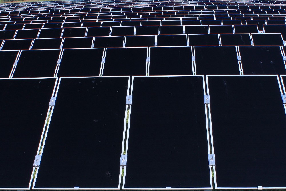
在过去几年中,原子层沉积(ALD)已成为微电子设备生产中沉积高 K(高导通率)栅极氧化物、阻挡层和种子层的常用工艺。在光伏领域,ALD 被用于缓冲层和背面钝化。
由于工艺开发的复杂性,工艺监测和控制对于加快开发周期、降低成本和了解众多工艺参数之间的相互作用至关重要。

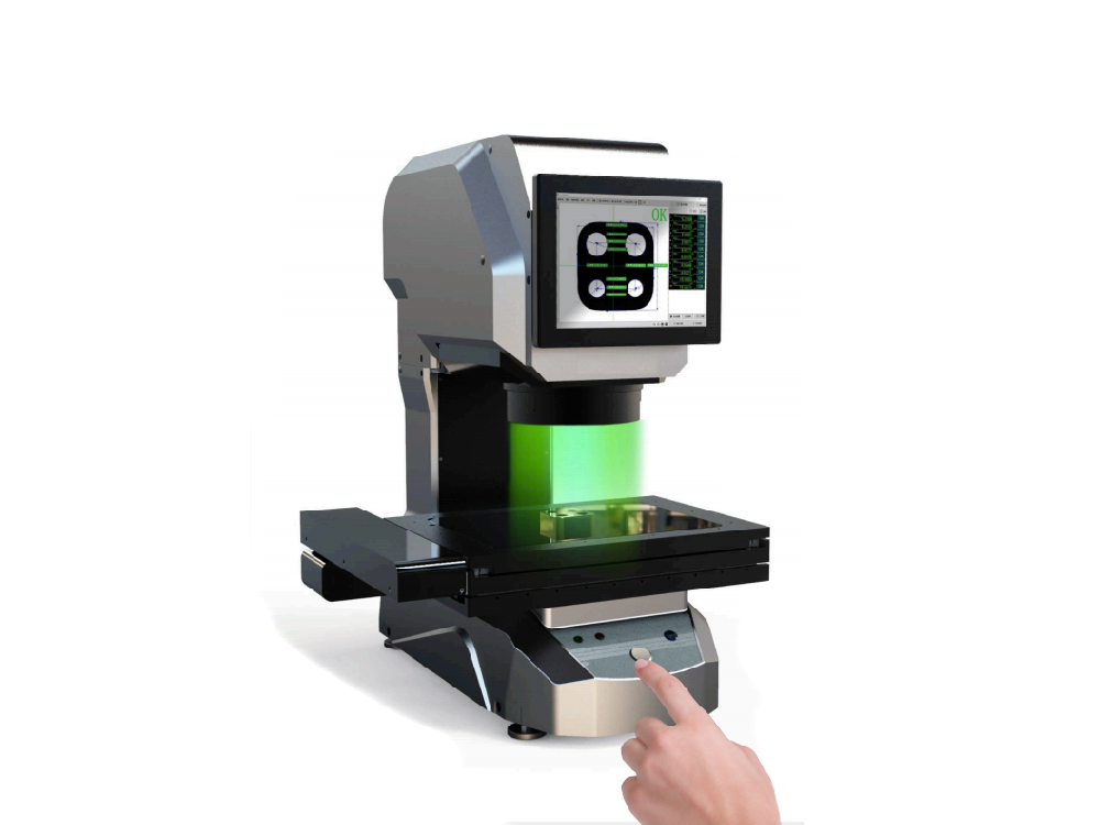
在原子层沉积 (ALD) 过程中,原位工具可用于薄膜厚度和蚀刻控制、薄膜叠层分析和温度均匀性。LayTec原位工具应用于ALD反应堆:
- 薄膜厚度监测
- 蚀刻控制
- 薄膜叠层分析分级
- 温度均匀性监控
LayTec 的 EpiTT 现场测量系统已成功应用于太阳能电池应用的空间 ALD 工艺和下一代闪存的多层电介质 ALD 制造。
英文:
Over the last few years, Atomic Layer Deposition (ALD) has become a common process in the production of microelectronic devices to deposit high-k (high permittivity) gate oxides, barrier and seed layers.
In photovoltaics, ALD is applied for buffer layers and backside passivation. Due to the complexity of the process development, process monitoring and control are crucial in order to accelerate development
cycles, reduce costs and understand the interaction of numerous process parameters.
During Atomic Layer Deposition (ALD), in-situ tools are used for film thickness and etching control, film stack analysis and temperature homogeneity.LayTec in-situ tools are applied in ALD reactors for:
• Film thickness monitoring
• Etching control
• Film stack analysis grading
• Monitoring of temperature homogeneity
LayTec’s EpiTT in-situ metrology systems are already successfully applied in spatial ALD processes for solar cell applications and in ALD manufacturing of multi-layer dielectrics for next-generation
flash memories.
电话
021-68680803
邮 箱:jianping.zheng@dayk.com.cn
手 机:13816545905
地 址:(华东)上海市浦东新区沪南路2419弄31号906室(复地万科活力城A906室) (华南)广东省东莞市御豪轩科技大厦一栋405
Copyright © 2018-2020 上海岱珂机电设备有限公司 All Rights Reserved. 技术支持:盘胧网 备案号:沪ICP备19023602号-1