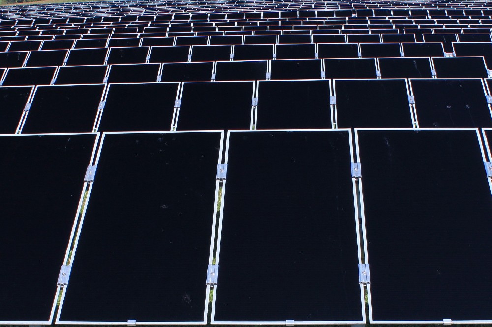
在聚光光伏中,基于III - V族化合物半导体材料的多结太阳能电池可以实现高达44 %的高效率。从大面积收集的太阳光集中在小面积太阳能电池上。LayTec原位测量系统使您可以跟踪MOCVD或MBE生长多层太阳能电池结构的所有工艺步骤。这些系统监控:

● 层厚度和生长速率 ● 表面形貌
● 表面化学计量比 ● 薄膜应变和晶片弓出
● 薄膜成分 ● 真晶片温度
● 掺杂浓度
以及其他关键参数。
对于工业CPV应用,需要结合实时统计过程控制对增长进行鲁棒分析。 针对行业需求,采用LayTec公司的Epi TT和Epi Curve ® TT产品族,结合Epi Guard ®软件包。这些原位系统提供了对生长参数的全面和稳健的监测。发射率校正测温( ECP )已成为这些计量系统的支柱,因为晶片的质量、成分和掺杂水平高度依赖于晶片表面温度,因为它是由Lay Tec公司的集成ECP模块在III - V、Si或Ge衬底上测量的。

高性能CPV外延的第二个关键是生长过程中所有层的精确厚度监测。在405nm、633nm和950nm处同时进行反射率测量,提供了关于层厚度、表面形貌和界面质量的信息。特别是较短的波长( 405 nm )已经被广泛用于表征AlInP工艺过程中的工艺窗口。
另一个关键参数是生长过程中和生长后的晶片弓形。Ⅲ-Ⅴ族化合物在Ge上的异质外延导致了晶片的显著弯曲。研究发现,在这些应用中,经过有意的缓冲器弛豫后,变体生长的曲率是强非球面的。LayTec公司的 高级分辨率( AR )曲率技术 使用户能够区分球面曲率和非球面性。由此产生的信号有助于在外延过程的早期和决定性阶段优化缓冲层的生长及其弛豫。
对于集中型多结太阳电池的研究和开发,直接实时获取界面化学计量比和掺杂水平对于深入理解外延生长过程中发生的效应是必不可少的。利用Lay Tec公司的EpiRAS ® TT中的光学方法- -反射各向异性光谱( RAS ),可以实现这种控制。其中一个技术挑战是在IV族Ge衬底上生长低缺陷的III - V族半导体结构。在这里,EpiRAS ® TT有助于在整个MOCVD过程中控制异质结构的关键生长参数。该计量系统可以避免在Ge界面III - V处形成初始反相边界,并提供宽范围的光谱反射测量以确定三元组分和生长速率,RAS信号测量掺杂水平,最后,发射率校正的高温计用于精确的温度监测。 . . . 等等
通过原位监测提升三结成品率
《化合物半导体》 杂志发表了一篇文章,报道了Lay Tec公司的原位计量工具在聚光光伏电池开发和生产中的应用。
英文:
In concentrated photovoltaics, high efficiency of up to 44% can be achieved nowadays with multi-junction solar cells based on III-V compound semiconductor materials. Sunlight collected from a large area is focused on small area solar cells. LayTec in-situ metrology systems enable you to follow all the process steps during MOCVD or MBE growth of multi-layer solar cell structures. These systems monitor:
• Layer thickness and growth rate • Surface morphology
• Surface stoichiometry • Film strain and wafer bowing
• Film composition • True wafer temperature
• Doping concentration
and other key parameters.
For industrial CPV applications, robust analysis of the growth combined with a real-time statistical process control is needed. For industrial requirements, LayTec’s EpiTT and EpiCurve® TT product families in combination with the EpiGuard® software packageare applied. These in-situ systems provide a comprehensive and robust monitoring of growth parameters. Emissivity corrected pyrometry (ECP) has become the backbone of these metrology systems because crystalline quality, composition, and doping level highly depend on wafer surface temperature as it is measured on III-V, Si or Ge substrates by LayTec’s integrated ECP modules.
The second key to high performance CPV epitaxy is the precise thickness monitoring of all layers during growth. Simultaneous reflectance measurement at 405 nm, 633 nm and 950 nm provide information on layer thickness, surface morphology and interface quality. In particular the shorter wavelength (405 nm) is widely used for characterization of AlInP process window already during the process.
A further critical parameter is the wafer bow during and after growth. The heteroepitaxy of the III-V compounds on Ge leads to a significant bow of the wafer. It was found that the curvature in these applications is strongly aspheric after intentioned buffer relaxation for metamorphic growth. LayTec’s advanced resolution (AR) curvature technology enables the user to distinguish between spherical curvature and asphericity. The resulting signal helps to optimize the buffer growth and its relaxation at early and decisive stages of the epitaxial process.
For research and development of concentrated multi-junction solar cells, a direct real-time access to interface stoichiometry and doping levels is indispensable for deep understanding of the effects that occur during the epitaxial growth. This kind of control is possible with Reflectance Anisotropy Spectroscopy (RAS) – an optical method applied in LayTec’s EpiRAS® TT. One of the technological challenges is the growth of low defect III-V semiconductor structures on co-valent group IV Ge substrates. Here, EpiRAS® TT helps control key growth parameters of the heterostructures throughout MOCVD process. The metrology system enables avoiding initial antiphase boundary formation at the III-V of Ge interface and provides wide-range spectral reflection measurements to determine ternary composition and growth rate, RAS signal to measure the doping level and, last but not least, the emissivity corrected pyrometry for an accurate temperature monitoring. ...more
Boosting triple-junction yield with in-situ monitoring
Compound Semiconductor Magazine published an article that reports about the application of LayTec’s in-situ metrology tools for development and production of concentrator photovoltaic cells.
电话
021-68680803
邮 箱:jianping.zheng@dayk.com.cn
手 机:13816545905
地 址:(华东)上海市浦东新区沪南路2419弄31号906室(复地万科活力城A906室) (华南)广东省东莞市御豪轩科技大厦一栋405
Copyright © 2018-2020 上海岱珂机电设备有限公司 All Rights Reserved. 技术支持:盘胧网 备案号:沪ICP备19023602号-1